
Packaging Roadmaps Are Becoming Harder to Predict
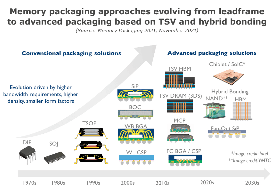 Advanced packaging is becoming one of the most important parts of the semiconductor supply chain, but it is also becoming harder to forecast. The latest signal came from concerns that some major memory customers may delay broader adoption of hybrid bonding, a key chip stacking technology. Shares of BE Semiconductor fell 6.7% after reports suggested that adoption timing may be pushed out by key customers, even though the company has benefited strongly from advanced packaging demand this year.
This does not mean advanced packaging demand is weakening. In fact, the opposite is true. Earlier this year, BE Semiconductor reported that first quarter order bookings rose 104.5% year over year to €269.7 million, supported by growing demand for hybrid bonding and advanced packaging tools. (Reuters)
The issue is timing.
Why Packaging Roadmaps Are Hard to Forecast
Advanced packaging roadmaps depend on more than demand. They depend on technical readiness, yield, customer qualification, cost, production standards, and adoption timing across multiple chipmakers.
Hybrid bonding is a good example. The technology enables extremely dense chip stacking by directly connecting chips with very fine interconnects. That can improve bandwidth, power efficiency, and package density, which makes it important for future memory, AI, and high performance computing products.
However, moving from technical promise to high volume manufacturing is difficult. Hybrid bonding requires precise alignment, clean surfaces, strong process control, and careful handling. Small process issues can affect yield and reliability.
That means adoption can slow even when the long term direction remains clear.
Why Delays Matter for Inventory Planning
Packaging delays can affect the entire supply chain.
If a company expects a certain packaging technology to scale quickly, it may plan product timing, qualification, and procurement around that assumption. If adoption slows, wafers, die, substrates, or related inventory may sit longer than expected before final assembly.
That creates a different kind of inventory risk.
The risk is not only whether supply exists. It is whether supply is ready to move through the next stage of production at the expected time.
For OEMs and EMS providers, this matters because finished component availability depends on more than wafer output. A wafer still needs to become known good die. Die still need packaging. Packages still need testing, qualification, and approval before they become usable supply.
The Role of Die and Wafer Banking
When packaging roadmaps become less predictable, die and wafer banking become more relevant.
Securing wafers or die earlier in the lifecycle gives companies flexibility. Inventory can be preserved upstream while packaging capacity, qualification timelines, or product requirements become clearer.
This is especially important for long lifecycle industries such as aerospace, defense, medical, industrial, and automotive manufacturing. These sectors often cannot redesign quickly when component availability shifts. They need continuity, traceability, and confidence that critical semiconductor supply can be preserved over time.
Why Storage Becomes More Technical
Storing wafers and die is different from storing finished packaged components.
Unfinished semiconductor inventory can be sensitive to contamination, moisture, electrostatic discharge, temperature variation, and handling conditions. If storage is not controlled properly, inventory secured early may lose value before it can be packaged or deployed.
Effective semiconductor storage protects inventory through controlled humidity, ESD protection, stable environmental conditions, documented custody, and traceability. For die and wafer banking, storage is not just a warehouse function. It is part of preserving future optionality.
The Bigger Lesson
Advanced packaging remains a critical growth area, but the path from roadmap to volume production is not always linear. Demand can be strong while adoption timing remains uncertain.
That distinction is important.
Packaging capacity, technology adoption, and qualification timelines now shape when semiconductor supply becomes usable. As the industry relies more heavily on chiplets, hybrid bonding, high bandwidth memory, and advanced integration, manufacturers will need to think beyond finished components.
Packaging roadmaps are becoming harder to predict. That makes upstream planning, die and wafer banking, and controlled semiconductor storage more important parts of long term supply strategy.